
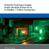
 The OCD spectroscopy approach. Though practical, it has limited spatial and spectral resolution and long scan times. (b, d) The LHSI approach developed by the research team, with a shorter scanning time and much higher spatial and spectral resolution. Each square in the grid shown in (d) corresponds to an observed “pixel.” Credit: Yoon et al., doi: 10.1117/1.JMM.21.2.021209")
Semiconductor fabrication technology, used commonly in modern electronics, has been steadily advancing for decades. Today, semiconductor devices have shrunk to miniature sizes but are capable of performing unprecedented complex functions. However, manufacturing semiconductors at the scale of a few nanometres has its fair share of technical challenges. For semiconductor devices to operate as intended, manufacturers need to guarantee the uniformity of what is known as “critical dimension” (CD). Manufacturing processes should be capable of accurately replicating the finest details of semiconductor structures down to the CDs, since even minor imperfections could cause devices to malfunction.
Unfortunately, one of the main problems of manufacturing ever-smaller semiconductor devices is that there are currently no fast, reliable and accurate techniques available to measure CD uniformity in cells, chips and wafers. Even though technologies like transmission electron microscopy and atomic force microscopy offer high spatial resolution, their scanning speed is too slow to make their application feasible for high-speed manufacturing. Fast measurement methods do exist, such as optical critical dimension (OCD) spectrometry (which measures uniformity in semiconductor devices by analysing the spectrum of light reflected off their surface). But such methods often have a low spatial resolution, putting them at a disadvantage.
Against this backdrop, a team of researchers led by Dr Myungjun Lee, head of the Inspection Solution Group at Samsung Electronics, recently developed a novel approach called “line-scan hyperspectral imaging” (LHSI). This method can potentially solve the issue of speed and resolution in measuring CD uniformity. The LHSI system is designed to deliver a better resolution than OCD along with a much higher throughput. The key difference between OCD and LHSI is the way in which the surface of the semiconductor is scanned. In OCD, the system focuses a beam of light to produce a bright spot on the wafer. The reflected light is then captured by a spectrometer and the acquired spectrum is analysed. Because the bright spot is rather large, OCD systems have a low resolution, making it hard to visualize small details in the semiconductor’s structure.
In contrast, the LHSI system illuminates the wafer’s surface with a narrow rectangular beam, an approach known as “line scan.” The reflected rectangular beam is relayed into a hyperspectral module, which consists of an arrangement of mirrors, slits, gratings and cameras. The gratings spatially decompose the incoming beam into its constituent frequencies, which are then captured by cameras optimised for different spectral ranges.
The LHSI approach allows the cameras to capture the spectral information of each vertical “pixel” of the scanning rectangular beam in one shot. As a result, a large amount of data can be generated quickly, speeding up the CD uniformity measurements. “Our system enables the simultaneous collection of massive amounts of spectral and spatial information with an extremely large field of view of 13 × 0.6 mm2”, says Dr Lee. “Additionally, our method has an improved throughput of up to 10,000 times compared to the standard OCD method.”
In addition to its speed, the LHSI system offers a spatial resolution of 5 μm and a spectral resolution of 0.25 nm over a wide range of wavelengths (350–1100 nm). This allowed the researchers to clearly observe fine details on various semiconductor devices, outperforming other conventional approaches by a remarkable margin. “We believe that there is currently no technology other than LHSI that can be used to analyse CD uniformity at such high levels of throughput and resolution”, says Dr Lee. “It could be the tool we need to overcome current measurement limitations in the field of high-volume semiconductor manufacturing. However, even though we successfully demonstrated the potential of LHSI, the critical modules, including a more stable light source, higher sensitivity cameras, higher precision optics etc. need to be further improved by suppliers.”
Overall, these results suggest that LHSI is a promising solution to one of the pressing problems in semiconductor manufacturing. Perfecting this technology further will help accelerate semiconductor development and fabrication processes, reducing their costs and enhancing the performance of the electronic devices we rely on so much today.


 cells in treated tumour cells")


 generate an RGB video image, the newly developed laparoscope (left) uses a multispectral camera. This also makes it possible to visualise functional properties of the tissue. Source: Leonardo Ayala / DKFZ")
